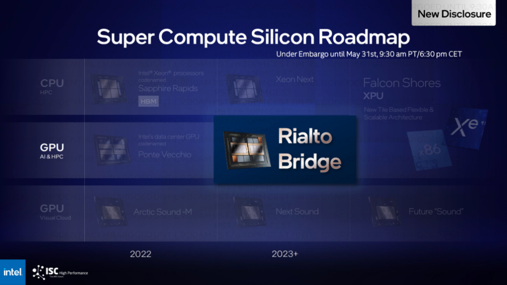
The Ponte Vecchio, also known as Rialto Bridge, is the next-generation successor from Intel to their flagship Xe GPU. The new graphics chip is aimed at AMD’s CDNA and NVIDIA’s CUDA processors in the next generation of AI and HPC data centres.
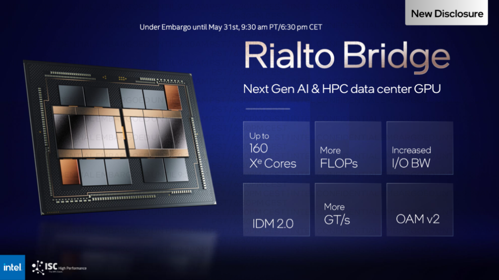
The Intel Rialto Bridge GPU is an improved version of the Ponte Vecchio GPU, featuring additional cores, flops, bandwidth, and GT/s. Intel hasn’t revealed many details about Rialto Bridge, but it claims it will have up to 160 Xe cores. We don’t know if these are the same cores as the present Ponte Vecchio GPUs or if they’re based on a whole new architecture, but the latter appears to be the case.

Today we are announcing our successor to this powerhouse data centre GPU, code-named Rialto Bridge. By evolving the Ponte Vecchio architecture and combining enhanced tiles with next process node technology, Rialto Bridge will offer significantly increased density, performance, & efficiency, while providing software consistency.
The Rialto Bridge is named after the same-called bridge in Venice, Italy, which is the oldest of the four bridges that span the Grand Canal
So it was with Ponte Vecchio, and it appears that the following generation, which will follow Rialto, will also be named after a famous bridge. Intel’s Rialto Bridge GPU, which is aimed at AMD CDNA and NVIDIA CUDA accelerators, will power the next generation of AI and HPC Data Center solutions, according to Intel.
Only the Rialto Bridge GPU will have up to 160 Xe cores in its brand new OAM v2 form factor is known in terms of specifications. Apart from the specifications, Intel also provides us with a first peek at the chip itself, and there are a few things we can look at. The GPU’s GPU dies layout is the most significant modification. The Rialto Bridge GPU has 8 16 Xe-HPC dies, each with 8 Xe cores for a total of 128 cores or 16,384 ALUs, whereas the Ponte Vecchio GPU has 16 Xe-HPC dies, each with 8 Xe cores for a total of 128 cores or 16,384 ALUs. So each die should have 20 Xe cores, for a total of 160 Xe cores across the eight dies.
The rest of the Rialto Bridge GPU structure is similar to the Ponte Vecchio GPU, with two Xe Link Tiles, eight HBM Tiles (HBM3), and four HBM stacks tied to each compute tile (4 Xe HPC dies). There are also passive die stiffeners around the Compute Tiles, and the Xe Link and HBM3 Tiles are connected to the Compute Tile using an EMIB Tile. The Compute Tile communicates with the rest of the Xe Dies through the Foveros chip interface.
The exact variety of each tile is unknown at this time, however, it should be based on the new Foveros Omni (3rd Gen) design. Also, the Rambo Cache tile appears to be missing, but considering the increased die size of each Compute tile, it’s plausible that the cache is now featured on the Compute tile itself rather than on its tile.

In terms of performance, Intel hasn’t provided any specific figures, merely stating that we may expect higher FLOPs, GT/s, and bandwidth. The improved HBM3 memory dies should be responsible for the higher bandwidth. The Ponte Vecchio GPUs already have up to 128 GB of VRAM, so we should see that on the Rialto Bridge GPUs as well, but Intel could stack it even higher.
Following is the full Intel Rialto Bridge die configuration that we can dissect at the moment:
· 8 Xe HPC (internal/external)
· 2 Xe Base (internal)
· 11 EMIB (internal)
· 2 Xe Link (external)
· 8 HBM (external)
Intel hasn’t announced a release date or provided any data about the process node for the Rialto Bridge GPU, but we’ll probably learn more about it in mid-2023 when it’s sampled to the first customers, with a launch date set for late 2023 or the first half of 2024.
also read:
Billionaires including Elon Musk, Jeff Bezos, Bill Gates, and Larry Page lose around $140 billion


