Samsung Electronics has previously said that mass production of the 3GAE (early 3nm gate-all-around) technique will begin this quarter (that is, these few weeks). However, it was previously claimed in the industry that Samsung’s 3nm yield rate was just 20-30%, which might slow down mass manufacturing and raise industry concerns.
According to Digitimes, Samsung’s 3nm yield problem has been fixed and that the 3nm GAA process will be mass-produced on time.
During its first-quarter conference call, Samsung assured shareholders that the company is on pace. Samsung Electronics is attempting to reassure investors following reports of yield issues at its foundry.
Samsung also stated that the 5nm process has reached a mature stage of mass production and that the production capacity of 4nm chips will soon begin to improve. “Although the output expansion of the 4nm process was delayed in the early stage, it is now focusing on stability., into the expected yield improvement curve.”
“By improving the node development system for the 3nm process, Samsung now has a verification process for each development stage,” Samsung also said, emphasizing that this will help shorten production ramps, improve profitability, and ensure a more stable supply.

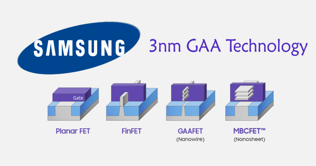
Samsung has chosen to forsake FinFET transistor technology, the world’s first GAA transistor technique, in the next 3nm node, whilst TSMC’s 3nm process will continue to use the old process
GAA is a novel type of gate-all-around transistor, according to Samsung, that can greatly improve transistor performance by employing nanosheet devices to construct MBCFETs (Multi-Bridge-Channel FETs).
According to Samsung, the 3nm GAA technology improves logic area efficiency by more than 45 percent, reduces power consumption by 50 percent, and boosts performance by roughly 35 percent when compared to the 7nm production process. On paper, it outperforms TSMC with its 3nm FinFET process.


Samsung 3nm yields are still in the 15% range, and anything Samsung claims to the contrary, are lies, by their own admission. They have repeatedly lied about their 5nm, 4nm, and 3nm yields for years, and after recently getting caught lying, admitted they were lying, and now suddenly we are supposed to believe they have miraculously improved yields.