In late 2025, Taiwan Semiconductor Manufacturing Corp. plans to begin high-volume manufacture of chips utilising its N2 (2 nm-class) process technology, with the first batch expected to arrive in early 2026. Apple and Intel will be the first customers to use N2, according to two media stories and financial community sources.
Apple has been TSMC’s greatest revenue contributor for nearly a decade, so it’s no surprise that it’ll be an early adopter of N2. Intel plans to employ TSMC’s services to manufacture graphics processing units (GPUs) and other SoCs, two applications that benefit from leading-edge nodes. According to rumours from DigiTimes and UDN, Intel will be one of the early adopters of N2. Intel will also swiftly become one of the foundry’s key customers, given its volume.
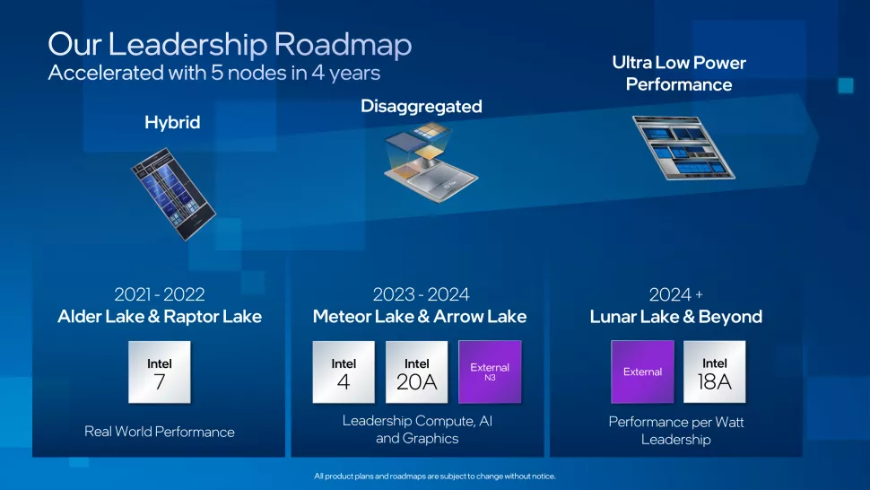
It’s unknown which of Apple’s system-on-chips (SoCs) will employ the N2 chips when the first batch is delivered in early 2026. Meanwhile, experts at China Renaissance Securities believe Intel would adopt TSMC’s N2 for its codenamed Lunar Lake processor’s graphics tile.
AMD, Broadcom, Nvidia, and MediaTek have all announced that they will employ TSMC’s N5 family of nodes (N5, N5P, N4, N4P, N4X)

Nvidia will use a unique 4N production process for its Hopper and probably Ada Lovelace GPUs, but MediaTek has previously announced its N5-based Dimensity 8000/8100 application processors and N4-based Dimensity 9000 SoC. The 5 nm technology will also be used in AMD’s Genoa and Raphael processors.
According to the DigiTimes article, all of these firms are now in discussions with TSMC about the capacity allocation for N3-capable capacities beginning in late 2023 or early 2024. Furthermore, these firms are likely to begin discussions for N2-capable allocations next year, but they will almost probably embrace N2 far later than Apple and Intel.
Years after Samsung’s 3GAE (2023) and more than a year after Intel’s 20A, TSMC’s N2 will be the foundry’s first technology to utilise gate-all-around field-effect transistors (GAAFET) (2024). So yet, the world’s largest contract chipmaker hasn’t said much about what to expect from N2 in terms of power, performance, or area/transistor density improvements over N3.
However, given that this would be a brand-new node, tangible gains over its predecessors are fair to expect. The new fabrication technique will continue to use 0.33 numerical aperture extreme ultraviolet (EUV) lithography scanners. Intel’s 18A, on the other hand, will use ASML’s Twinscan EXE EUV scanners with High-NA (0.55NA).
Also Read:
TSMC crosses Revenues of Smartphones with its PC and Server chips


