In a new research paper published by the green team, a mysterious NVIDIA GPU known as GPU-N has been revealed, which could be the first look at the next-gen Hopper GH100 chip (as discovered by Twitter user, Redfire).
The research paper ‘GPU Domain Specialization via Composable On-Package Architecture’ discusses a next-generation GPU design as the most practical solution for boosting Deep Learning performance by maximizing low-precision matrix math throughput. The ‘GPU-N’ and its COPA designs, as well as their possible specifications and simulated performance results, have been discussed.
134 SM units are believed to be included in the ‘GPU-N.’ (vs 104 SM units of A100). This brings the total number of cores to 8576, which is a 24% increase over the present Ampere A100 solution. The chip’s theoretical clock speed is 1.4 GHz, which is the same as the Ampere A100 and Volta V100 (not to be confused as the final clocks).
Other features include a 60 MB L2 cache, which is a 50% improvement over the Ampere A100, and a 2.68 TB/s DRAM bandwidth that can scale up to 6.3 TB/s. The HBM2e DRAM has a capacity of 100 GB, which can be increased to 233 GB using COPA implementations. It’s built around a 6144-bit bus interface with 3.5 Gbps clock speeds.
| Configuration | NVIDIA V100 | NVIDIA A100 | GPU-N |
| SMs | 80 | 108 | 134 |
| GPU frequency (GHz) | 1.4 | 1.4 | 1.4 |
| FP32 (TFLOPS) | 15.7 | 19.5 | 24.2 |
| FP16 (TFLOPS) | 125 | 312 | 779 |
| L2 cache (MB) | 6 | 40 | 60 |
| DRAM BW (GB/s) | 900 | 1,555 | 2,687 |
| DRAM Capacity (GB) | 16 | 40 | 100 |
In terms of performance, the ‘GPU-N’ (probably Hopper GH100) generates 24.2 TFLOPs of FP32 (a 24 percent increase over A100) and 779 TFLOPs of FP16 (a 2.5x increase over A100), which seems very near to the 3x gains rumored for GH100 over A100. The FP32 performance of the Instinct MI250X accelerator is less than half that of AMD’s cDNA 2 ‘Aldebaran’ GPU (95.7 TFLOPs versus 24.2 TFLOPs), however, the FP16 performance is 2.15x higher.
NVIDIA’s H100 accelerator would be based on an MCM solution and use TSMC’s 5nm process node, according to previous information. Hopper is expected to have two next-generation GPU modules, totalling 288 SM units. We can’t give an exact number of cores because we don’t know how many are in each SM, but if it sticks to 64 cores per SM, we’ll have 18,432 cores, which is 2.25x more than the full GA100 GPU configuration. NVIDIA could also use more FP64, FP16, and Tensor cores in its Hopper GPU to greatly improve performance. And that will be required to compete with Intel’s Ponte Vecchio, which is expected to include 1:1 FP64.
The final configuration is likely to have 134 of the 144 SM units activated on each GPU module, implying that we’re looking at a single GH100 chip in action. However, without GPU Sparsity, NVIDIA is unlikely to achieve the same FP32 or FP64 Flops as MI200.
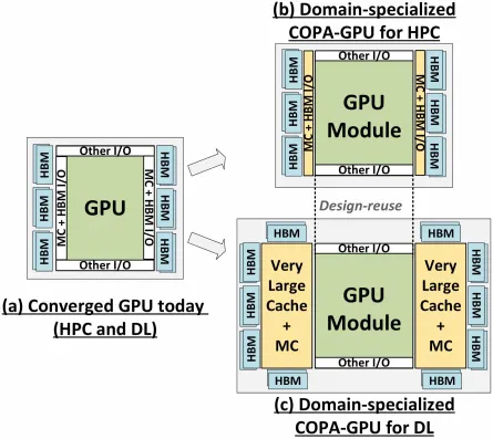
NVIDIA, on the other hand, may have a hidden weapon in the form of Hopper’s COPA-based GPU implementation. NVIDIA mentions two Domain-Specialized COPA-GPUs based on next-generation architecture, one for HPC and the other for DL. The HPC variant uses a relatively normal method, with an MCM GPU and HBM/MC+HBM (IO) chipsets, but the DL variation is where things start to get interesting. The DL version includes a large cache on a separate die that is coupled to the GPU modules.
| Architecture | LLC Capacity | DRAM BW | DRAM Capacity |
| Configuration | (MB) | (TB/s) | (GB) |
| GPU-N | 60 | 2.7 | 100 |
| COPA-GPU-1 | 960 | 2.7 | 100 |
| COPA-GPU-2 | 960 | 4.5 | 167 |
| COPA-GPU-3 | 1,920 | 2.7 | 100 |
| COPA-GPU-4 | 1,920 | 4.5 | 167 |
| COPA-GPU-5 | 1,920 | 6.3 | 233 |
| Perfect L2 | infinite | infinite | infinite |
There are several variants with up to 960 / 1920 MB of LLC (Last-Level-Cache), up to 233 GB of HBM2e DRAM capacity, and up to 6.3 TB/s of bandwidth. These are all hypothetical, but given that NVIDIA has already discussed them, we could see a Hopper variant with such a design at GTC 2022.
NVIDIA Hopper GH100 ‘Preliminary Specs’:
| NVIDIA Tesla Graphics Card | Tesla K40 (PCI-Express) | Tesla M40 (PCI-Express) | Tesla P100 (PCI-Express) | Tesla P100 (SXM2) | Tesla V100 (SXM2) | NVIDIA A100 (SXM4) | NVIDIA H100 (SMX4?) |
| GPU | GK110 (Kepler) | GM200 (Maxwell) | GP100 (Pascal) | GP100 (Pascal) | GV100 (Volta) | GA100 (Ampere) | GH100 (Hopper) |
| Process Node | 28nm | 28nm | 16nm | 16nm | 12nm | 7nm | 5nm |
| Transistors | 7.1 Billion | 8 Billion | 15.3 Billion | 15.3 Billion | 21.1 Billion | 54.2 Billion | TBD |
| GPU Die Size | 551 mm2 | 601 mm2 | 610 mm2 | 610 mm2 | 815mm2 | 826mm2 | TBD |
| SMs | 15 | 24 | 56 | 56 | 80 | 108 | 134 (Per Module) |
| TPCs | 15 | 24 | 28 | 28 | 40 | 54 | TBD |
| FP32 CUDA Cores Per SM | 192 | 128 | 64 | 64 | 64 | 64 | 64? |
| FP64 CUDA Cores / SM | 64 | 4 | 32 | 32 | 32 | 32 | 32? |
| FP32 CUDA Cores | 2880 | 3072 | 3584 | 3584 | 5120 | 6912 | 8576 (Per Module) 17152 (Complete) |
| FP64 CUDA Cores | 960 | 96 | 1792 | 1792 | 2560 | 3456 | 4288 (Per Module)? 8576 (Complete)? |
| Tensor Cores | N/A | N/A | N/A | N/A | 640 | 432 | TBD |
| Texture Units | 240 | 192 | 224 | 224 | 320 | 432 | TBD |
| Boost Clock | 875 MHz | 1114 MHz | 1329MHz | 1480 MHz | 1530 MHz | 1410 MHz | ~1400 MHz |
| TOPs (DNN/AI) | N/A | N/A | N/A | N/A | 125 TOPs | 1248 TOPs 2496 TOPs with Sparsity | TBD |
| FP16 Compute | N/A | N/A | 18.7 TFLOPs | 21.2 TFLOPs | 30.4 TFLOPs | 312 TFLOPs 624 TFLOPs with Sparsity | 779 TFLOPs (Per Module)? 1558 TFLOPs with Sparsity (Per Module)? |
| FP32 Compute | 5.04 TFLOPs | 6.8 TFLOPs | 10.0 TFLOPs | 10.6 TFLOPs | 15.7 TFLOPs | 19.4 TFLOPs 156 TFLOPs With Sparsity | 24.2 TFLOPs (Per Module)? 193.6 TFLOPs With Sparsity? |
| FP64 Compute | 1.68 TFLOPs | 0.2 TFLOPs | 4.7 TFLOPs | 5.30 TFLOPs | 7.80 TFLOPs | 19.5 TFLOPs (9.7 TFLOPs standard) | 24.2 TFLOPs (Per Module)? (12.1 TFLOPs standard)? |
| Memory Interface | 384-bit GDDR5 | 384-bit GDDR5 | 4096-bit HBM2 | 4096-bit HBM2 | 4096-bit HBM2 | 6144-bit HBM2e | 6144-bit HBM2e |
| Memory Size | 12 GB GDDR5 @ 288 GB/s | 24 GB GDDR5 @ 288 GB/s | 16 GB HBM2 @ 732 GB/s 12 GB HBM2 @ 549 GB/s | 16 GB HBM2 @ 732 GB/s | 16 GB HBM2 @ 900 GB/s | Up To 40 GB HBM2 @ 1.6 TB/s Up To 80 GB HBM2 @ 1.6 TB/s | Up To 100 GB HBM2e @ 3.5 Gbps |
| L2 Cache Size | 1536 KB | 3072 KB | 4096 KB | 4096 KB | 6144 KB | 40960 KB | 81920 KB |
| TDP | 235W | 250W | 250W | 300W | 300W | 400W | ~450-500W |
also read:
AMD stock reports steady growth after a decline over the second half of this year